Infinity Fabric and Cache Coherence — How AMD and Apple Build Unified Memory
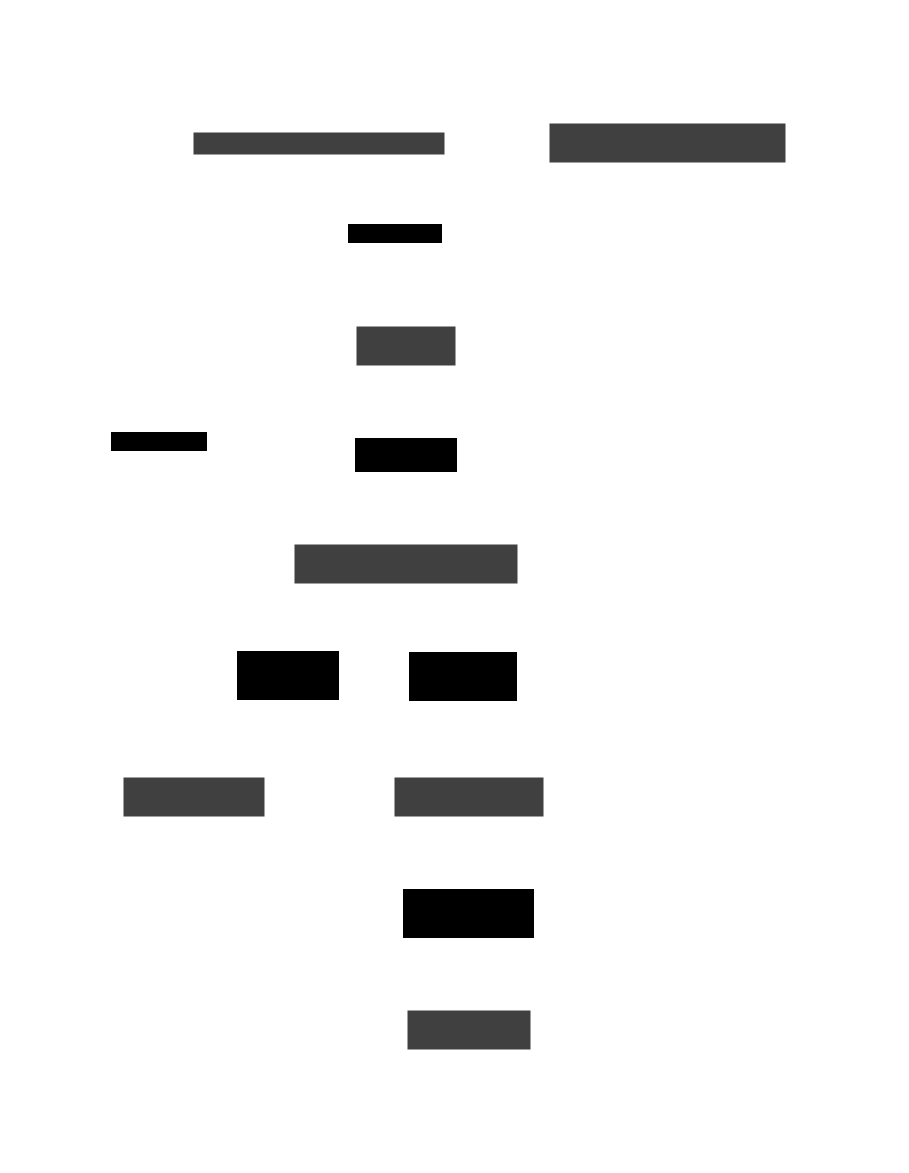
Every time your CPU writes to memory and your GPU reads from it — on the same APU, same SoC, same unified memory pool — there is a silent negotiation happening at nanosecond speed. Cache lines change state. Snoop probes traverse the fabric. Directories update. And somehow, after all of that, the GPU gets 42 instead of the stale 0 that main memory still holds.
This post is about the silicon that makes that work.
Part 1: Cache Coherence — The Problem
Before we talk about fabrics, we need to understand what they solve. Here is the fundamental problem:
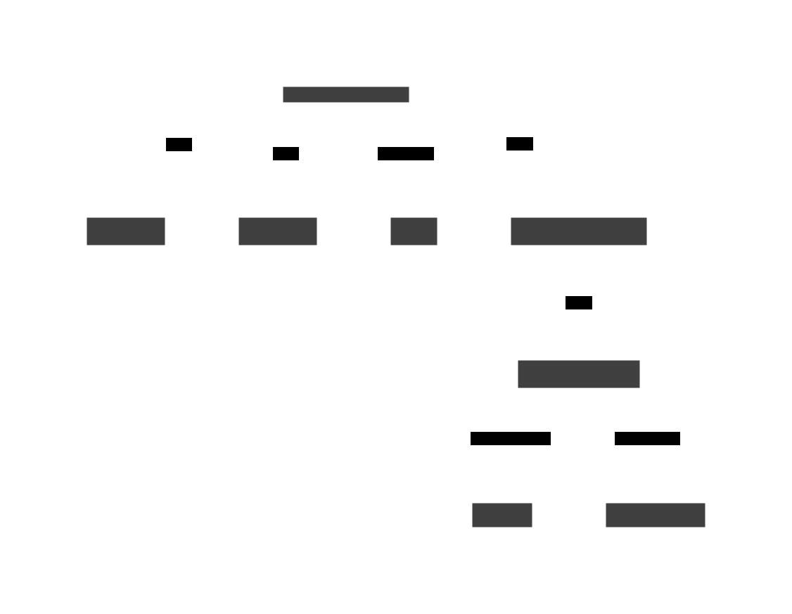
Without a coherence protocol, Core B reads 0 from DRAM — stale data. The CPU’s memory model breaks. Every multithreaded program becomes undefined behavior. This is not a theoretical problem; it is the reason your multi-core processor works at all.
The solution is a cache coherence protocol: a set of rules that governs what happens when one cache writes to an address that other caches might also hold. Every core, every GPU compute unit, every accelerator that shares a memory space participates in this protocol.
Part 2: MOESI — The Five-State Protocol
AMD uses the MOESI protocol across its entire product line — Ryzen, EPYC, and APUs. It extends the simpler 4-state MESI protocol with a critical fifth state: Owned (O).
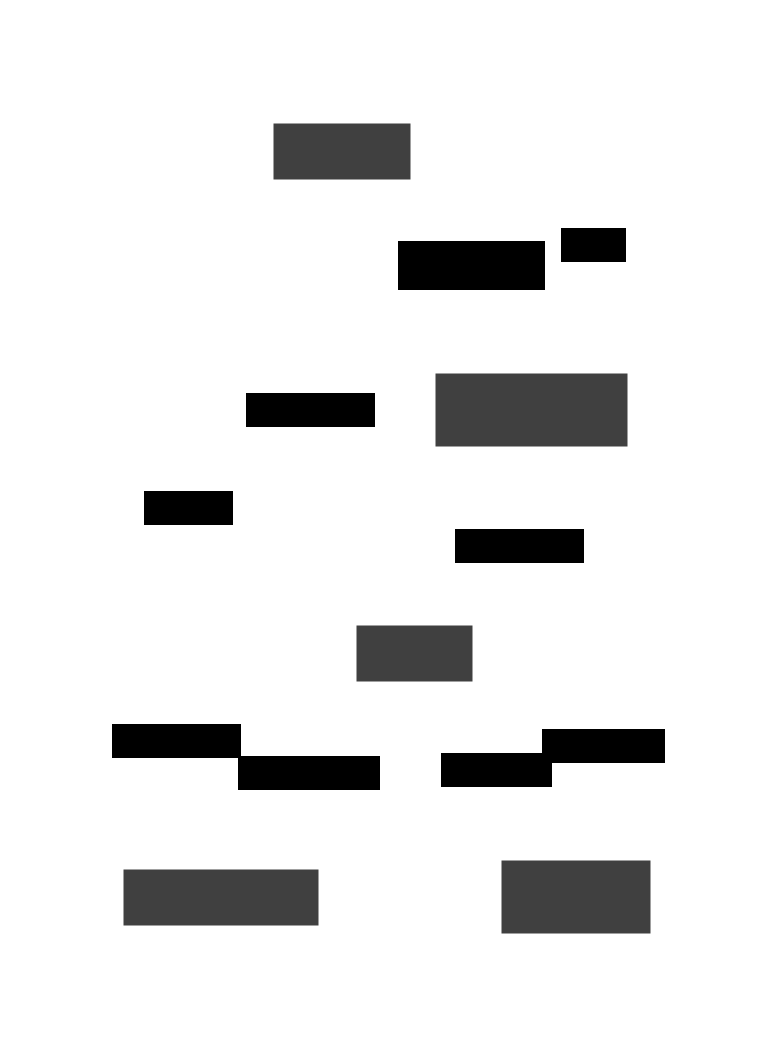
Here is what each state means in practice:
| State | Dirty? | Other copies? | Can write silently? | On eviction |
|---|---|---|---|---|
| M (Modified) | Yes | No | Yes | Must write-back |
| O (Owned) | Yes | Yes (Shared copies) | No | Must write-back |
| E (Exclusive) | No | No | Yes (upgrade to M) | Silent drop |
| S (Shared) | No | Possibly | No (invalidate first) | Silent drop |
| I (Invalid) | N/A | N/A | No (must fetch) | N/A |
Why the Owned State Matters
The Owned state is AMD’s secret weapon for producer-consumer workloads. Here is why.
In a standard MESI protocol (used by ARM’s base implementation and many embedded designs), when Core A holds a Modified (dirty) line and Core B wants to read it:
MESI flow:
1. Core B issues read request
2. Core A must write-back dirty data to DRAM  ← costly
3. Core A downgrades M → S
4. Core B reads from DRAM                     ← costly
5. Core B gets S state
Total: 1 write-back + 1 DRAM read
In MOESI:
MOESI flow:
1. Core B issues read request
2. Core A transitions M → O (keeps dirty data)   ← no write-back!
3. Core A sends dirty data directly to Core B     ← cache-to-cache
4. Core B gets S state
Total: 0 DRAM transactions
The savings are massive. A DRAM write-back costs ~80-90 ns on a typical DDR5 system. A cache-to-cache transfer over Infinity Fabric costs ~15-40 ns within the same CCD. For producer-consumer patterns — which describe approximately all multithreaded programs — MOESI eliminates the most expensive part of the coherence transaction.
Intel’s Alternative: MESIF
Intel chose a different optimization. Instead of allowing dirty sharing (the O state), Intel added the Forward (F) state:
| State | Description |
|---|---|
| F (Forward) | Clean. Designated responder for shared lines. Only one cache holds F at a time. |
When multiple cores share a cache line and a new core requests it, only the F-state cache responds. All other S-state caches stay silent. This eliminates redundant snoop responses without relaxing the rule that dirty data always has a single owner.
The trade-off: MESIF avoids the complexity of dirty sharing but still requires write-backs when dirty lines are shared. MOESI eliminates those write-backs at the cost of more complex ownership tracking.
How Coherence Scales: Snoop Filters and Directories
On a 4-core system, you can broadcast every coherence request to every core. It works. On a 128-core EPYC, broadcasting would saturate the interconnect.
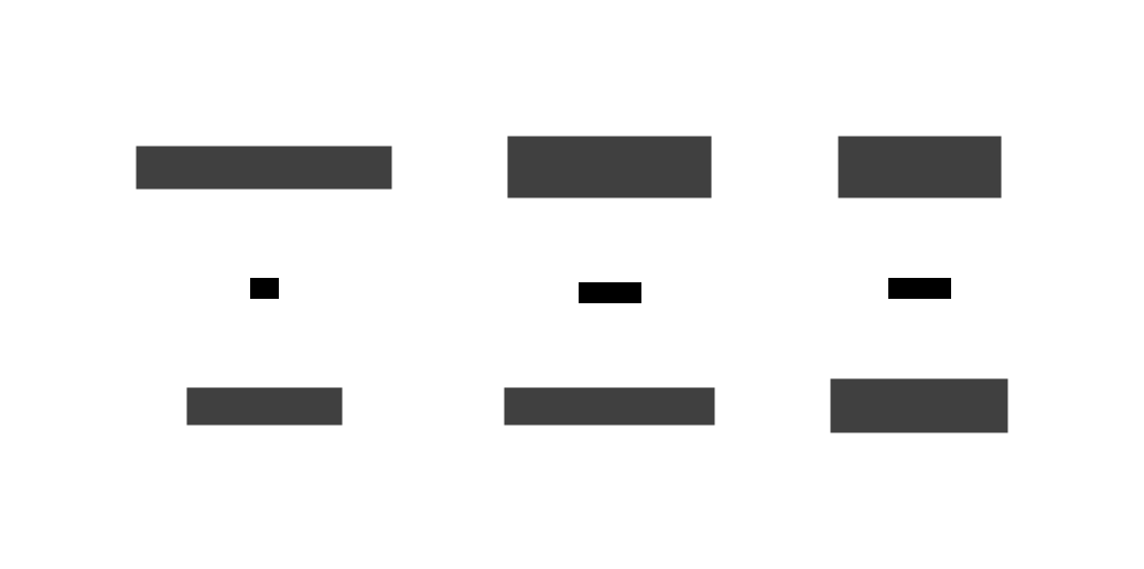
Modern AMD EPYC processors use a hybrid approach: MOESI with directory-based extensions. Each CCD maintains snoop-based MOESI coherence internally (fast, low-latency, ~8 cores sharing an L3). Cross-CCD traffic goes through the I/O Die’s directory structures, which track exactly which CCD holds each cache line. Instead of broadcasting to all CCDs, the directory sends targeted probes only to the relevant one.
The result: ~15 ns intra-CCD coherence latency, ~80-150 ns cross-CCD coherence latency. The 10x penalty is the price of scaling beyond a single L3 domain.
Part 3: Infinity Fabric — AMD’s Coherent Interconnect
Infinity Fabric is not a bus. It is not a ring. It is a packet-switched network-on-chip that connects every component in an AMD processor. It has two independent planes:
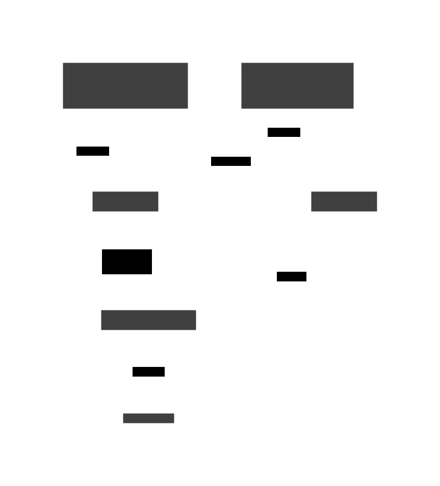
The Clock Triad: FCLK, UCLK, MCLK
Infinity Fabric performance depends on three clocks that must be kept in harmony:
| Clock | What it drives | Typical Zen 4 speed |
|---|---|---|
| FCLK | Infinity Fabric interconnect speed | 2000 MHz (IF 1:1 mode) |
| UCLK | Unified Memory Controller clock | 3000 MHz (DDR5-6000) |
| MCLK | DRAM bus clock | 3000 MHz (DDR5-6000, double data rate) |
The golden ratio for AMD systems has historically been FCLK:UCLK:MCLK at 1:1:1 — meaning the fabric, memory controller, and DRAM all run at the same base clock. When you overclock memory to DDR5-6400 (MCLK 3200, UCLK 3200) but leave FCLK at 2000, you enter 2:1 mode — the fabric runs at half the memory speed. This introduces a latency penalty of roughly 8-12 ns per transaction because the slower fabric becomes the bottleneck for coherence traffic.
Zen 5 relaxed this somewhat with better queue buffering, but the principle holds: fabric bandwidth gates everything.
The IOMMU and Heterogeneous Coherence
On an AMD APU, the GPU is not just another PCIe device. It sits on the same Infinity Fabric as the CPU cores, sharing the same memory controller. But the GPU uses its own page tables, its own virtual memory space. How does it read data the CPU wrote?
The IOMMU (I/O Memory Management Unit) bridges the gap:
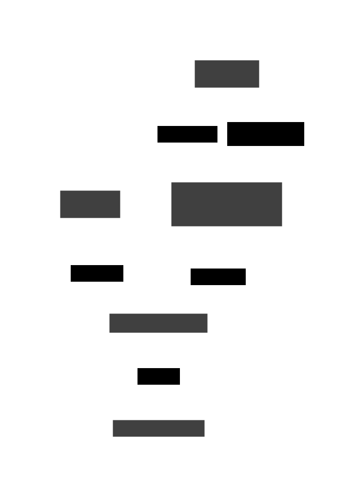
The key technology is ATS (Address Translation Services). Without ATS, the GPU would need the CPU to translate every address for it — a round-trip that kills performance. With ATS, the GPU’s IOMMU caches translations locally. The GPU requests a translation once, caches it in its own ATC (Address Translation Cache), and uses it for subsequent accesses.
But ATS alone does not solve coherence. The IOMMU also participates in the MOESI protocol: when the GPU reads an address through the IOMMU, the IOMMU issues a coherence probe on Infinity Fabric. If the CPU holds that line in Modified state, the probe triggers a cache-to-cache transfer — just like a CPU-to-CPU coherence transaction.
This is what makes an APU fundamentally different from a discrete GPU. On a discrete GPU:
- CPU writes to host DRAM (local, fast)
- GPU needs that data: PCIe copy from host DRAM to GPU VRAM (32 GB/s over PCIe 4.0 x16)
- GPU reads from VRAM (local, fast)
- Total latency: ~10 µs for the DMA transfer alone
On an APU:
- CPU writes to unified DRAM (local, fast)
- GPU reads from unified DRAM (local, fast, zero-copy)
- The IOMMU + Infinity Fabric handle address translation and coherence in hardware
- Total latency: ~100 ns for the coherence probe + DRAM access
That is a 100x latency improvement for cross-engine data sharing. No PCIe bus. No DMA engine. No separate VRAM pool. Just a coherence probe on the fabric.
Part 4: Apple’s Approach — The UltraFusion Monolith
Apple took a fundamentally different architectural bet. Instead of chiplets connected by a packet-switched fabric, Apple builds massive monolithic SoCs and, when they need more silicon than a single reticle limit allows, they fuse two dies with UltraFusion.
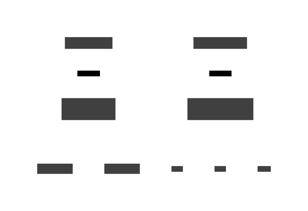
The difference is physical, not just philosophical:
| Dimension | Apple UltraFusion | AMD Infinity Fabric (Chiplet) |
|---|---|---|
| Physical medium | Silicon interposer embedded in package | Substrate traces (PCB-like routing) |
| Bandwidth | ~2.5 TB/s bidirectional | ~50-100 GB/s per IFOP link |
| Cross-die latency | Near-zero (nanoseconds) | ~80-150 ns |
| OS view | Single monolithic processor | NUMA nodes (multiple L3 domains) |
| Coherence scope | Single coherence domain | Directory-based across CCDs |
| Memory model | True UMA (uniform access) | NUMA (non-uniform, local vs remote) |
| Max scale | 2 dies (Ultra) | 8-12 CCDs per socket, multi-socket |
The System Level Cache (SLC)
Both architectures converge on a critical insight: you need a massive shared last-level cache to keep coherence traffic off the fabric. Apple calls it the System Level Cache. AMD calls it Infinity Cache (on RDNA GPUs) and the shared L3 per CCD (on Zen CPUs).
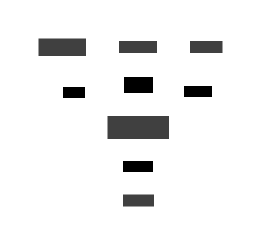
The SLC is the coherence traffic sponge. When the GPU reads a texture that the CPU just wrote, the data is often still in the SLC — no DRAM access needed. When the Neural Engine loads model weights, they sit in the SLC, shared by all engines. The SLC hit rate directly determines how much coherence traffic reaches DRAM.
Apple’s SLC is exclusive with respect to CPU caches: data evicted from L2 goes to the SLC, not duplicated. This avoids wasting cache capacity on redundant copies. The trade-off is slightly higher latency on L2 miss → SLC fill, but the capacity win is worth it for shared workloads.
Part 5: The Coherence Tax
Unified memory is not free. Every cross-engine access pays a coherence tax:
The numbers tell the story:
| Scenario | Latency | Bandwidth |
|---|---|---|
| APU: CPU → GPU (zero-copy, MOESI) | ~100 ns | ~51 GB/s (DDR5-6400) |
| Apple M4: CPU → GPU (SLC hit) | ~15 ns | ~120 GB/s (LPDDR5X) |
| Apple M4: CPU → GPU (SLC miss) | ~100 ns | ~120 GB/s |
| Discrete: CPU → GPU (PCIe 4.0 x16) | ~12 µs | ~32 GB/s |
| Discrete: CPU → GPU (PCIe 5.0 x16) | ~10 µs | ~64 GB/s |
The latency gap is 100-800x in favor of unified memory. The bandwidth comparison is more nuanced — DDR5-6400 at 51 GB/s shared across CPU and GPU can be a bottleneck compared to dedicated 272 GB/s GDDR6X on a discrete GPU. But for workloads where the CPU and GPU trade data back and forth (inference pipelines, video processing, ML training orchestration), the zero-copy advantage dominates.
The Bottom Line
Cache coherence is not an implementation detail. It is the architectural foundation that makes unified memory possible. MOESI’s Owned state eliminates write-backs when sharing dirty data. Infinity Fabric’s packet-switched SDF routes coherence probes at nanosecond speeds. Apple’s UltraFusion interposer makes cross-die coherence nearly free. The SLC absorbs coherence traffic before it hits DRAM.
The APU in my laptop — a Ryzen 7 7730U — runs the same MOESI protocol as a 128-core EPYC server. The same state machine. The same five letters. Just scaled down to a single die where cross-CCD directory lookups don’t exist because there is only one CCD.
Next time you pass a pointer from CPU to GPU on an APU and it just works, remember: a coherence probe traversed the fabric, a cache line changed state from Modified to Owned, a snoop filter decided who to notify, and somewhere in the IOMMU, an address was translated from GPU virtual to physical. All in under 100 nanoseconds.